- 您现在的位置:买卖IC网 > Sheet目录491 > NTMFS4927NCT3G (ON Semiconductor)MOSFET N-CH 30V SO8-FL
�� �
�
�NTMFS4927N,� NTMFS4927NC�
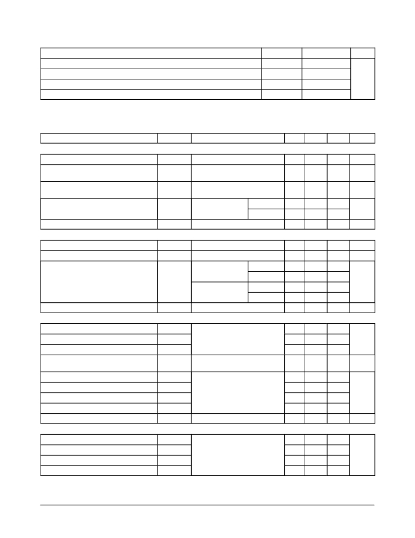
�THERMAL� RESISTANCE� MAXIMUM� RATINGS�
�Parameter�
�Junction� ?� to� ?� Case� (Drain)�
�Junction� ?� to� ?� Ambient� –� Steady� State� (Note� 3)�
�Junction� ?� to� ?� Ambient� –� Steady� State� (Note� 4)�
�Junction� ?� to� ?� Ambient� –� (t� ≤� 10� s)� (Note� 3)�
�Symbol�
�R� q� JC�
�R� q� JA�
�R� q� JA�
�R� q� JA�
�Value�
�6.0�
�46.3�
�136.2�
�20.7�
�Unit�
�°� C/W�
�3.� Surface� ?� mounted� on� FR4� board� using� 1� sq� ?� in� pad,� 1� oz� Cu.�
�4.� Surface� ?� mounted� on� FR4� board� using� the� minimum� recommended� pad� size.�
�ELECTRICAL� CHARACTERISTICS� (T� J� =� 25� °� C� unless� otherwise� specified)�
�Parameter�
�Symbol�
�Test� Condition�
�Min�
�Typ�
�Max�
�Unit�
�OFF� CHARACTERISTICS�
�Drain� ?� to� ?� Source� Breakdown� Voltage�
�Drain� ?� to� ?� Source� Breakdown� Voltage�
�(transient)�
�Drain� ?� to� ?� Source� Breakdown� Voltage�
�Temperature� Coefficient�
�V� (BR)DSS�
�V� (BR)DSSt�
�V� (BR)DSS� /�
�T� J�
�V� GS� =� 0� V,� I� D� =� 250� m� A�
�VGS� =� 0� V,� I� D(aval)� =� 8.4� A,�
�T� case� =� 25� °� C,� t� transient� =� 100� ns�
�30�
�34�
�24�
�V�
�V�
�mV/� °� C�
�Zero� Gate� Voltage� Drain� Current�
�I� DSS�
�V� GS� =� 0� V,�
�V� DS� =� 24� V�
�T� J� =� 25� °� C�
�T� J� =� 125� °� C�
�1.0�
�10�
�m� A�
�Gate� ?� to� ?� Source� Leakage� Current�
�I� GSS�
�V� DS� =� 0� V,� V� GS� =� ±� 20� V�
�±� 100�
�nA�
�ON� CHARACTERISTICS� (Note� 5)�
�Gate� Threshold� Voltage�
�V� GS(TH)�
�V� GS� =� V� DS� ,� I� D� =� 250� m� A�
�1.32�
�1.6�
�2.2�
�V�
�Negative� Threshold� Temperature� Coefficient�
�V� GS(TH)� /T� J�
�3.7�
�mV/� °� C�
�Drain� ?� to� ?� Source� On� Resistance�
�R� DS(on)�
�V� GS� =� 10� V�
�V� GS� =� 4.5� V�
�I� D� =� 30� A�
�I� D� =� 15� A�
�I� D� =� 30� A�
�5.8�
�5.7�
�9.6�
�7.3�
�12�
�m� W�
�I� D� =� 15� A�
�9.2�
�Forward� Transconductance�
�g� FS�
�V� DS� =� 1.5� V,� I� D� =� 15� A�
�40�
�S�
�CHARGES,� CAPACITANCES� &� GATE� RESISTANCE�
�Input� Capacitance�
�C� ISS�
�913�
�Output� Capacitance�
�Reverse� Transfer� Capacitance�
�Capacitance� Ratio�
�Total� Gate� Charge�
�Threshold� Gate� Charge�
�Gate� ?� to� ?� Source� Charge�
�Gate� ?� to� ?� Drain� Charge�
�Total� Gate� Charge�
�C� OSS�
�C� RSS�
�C� RSS� /�
�C� ISS�
�Q� G(TOT)�
�Q� G(TH)�
�Q� GS�
�Q� GD�
�Q� G(TOT)�
�V� GS� =� 0� V,� f� =� 1� MHz,� V� DS� =� 15� V�
�V� GS� =� 0� V,� V� DS� =� 15� V,� f� =� 1� MHz�
�V� GS� =� 4.5� V,� V� DS� =� 15� V;� I� D� =� 30� A�
�V� GS� =� 10� V,� V� DS� =� 15� V;� I� D� =� 30� A�
�366�
�108�
�0.118�
�8.0�
�1.6�
�3.1�
�3.1�
�16.0�
�0.237�
�pF�
�nC�
�nC�
�SWITCHING� CHARACTERISTICS� (Note� 6)�
�Turn� ?� On� Delay� Time�
�t� d(ON)�
�9.2�
�Rise� Time�
�Turn� ?� Off� Delay� Time�
�Fall� Time�
�t� r�
�t� d(OFF)�
�t� f�
�V� GS� =� 4.5� V,� V� DS� =� 15� V,�
�I� D� =� 15� A,� R� G� =� 3.0� W�
�25.5�
�14.0�
�4.4�
�ns�
�5.� Pulse� Test:� pulse� width� v� 300� m� s,� duty� cycle� v� 2%.�
�6.� Switching� characteristics� are� independent� of� operating� junction� temperatures.�
�http://onsemi.com�
�2�
�发布紧急采购,3分钟左右您将得到回复。
相关PDF资料
NTMFS4933NT1G
MOSFET N-CH 30V 232A SO8 FL
NTMFS4934NT1G
MOSFET N-CH 30V 147A SO8 FL
NTMFS4935NCT3G
MOSFET N-CH 30V SO8-FL
NTMFS4936NCT3G
MOSFET N-CH 30V 11.6A SO-8FL
NTMFS4937NT1G
MOSFET N-CH 30V 10.2A SO8 FL
NTMFS4939NT3G
MOSFET N-CH 30V 9.3A SO8 FL
NTMFS4941NT3G
MOSFET N-CH 30V 9A SO8 FL
NTMFS4943NT1G
MOSFET N-CH 30V 8.3A SO8 FL
相关代理商/技术参数
NTMFS4927NT1G
功能描述:MOSFET TRENCH 3.1 30V 9 Ohm NCH RoHS:否 制造商:STMicroelectronics 晶体管极性:N-Channel 汲极/源极击穿电压:650 V 闸/源击穿电压:25 V 漏极连续电流:130 A 电阻汲极/源极 RDS(导通):0.014 Ohms 配置:Single 最大工作温度: 安装风格:Through Hole 封装 / 箱体:Max247 封装:Tube
NTMFS4927NT3G
功能描述:MOSFET TRENCH 3.1 30V 9 Ohm NCH RoHS:否 制造商:STMicroelectronics 晶体管极性:N-Channel 汲极/源极击穿电压:650 V 闸/源击穿电压:25 V 漏极连续电流:130 A 电阻汲极/源极 RDS(导通):0.014 Ohms 配置:Single 最大工作温度: 安装风格:Through Hole 封装 / 箱体:Max247 封装:Tube
NTMFS4931N
制造商:ONSEMI 制造商全称:ON Semiconductor 功能描述:Power MOSFET 30 V, 246 A, Single N.Channel, SO.8 FL
NTMFS4931NT1G
制造商:ONSEMI 制造商全称:ON Semiconductor 功能描述:Power MOSFET 30 V, 246 A, Single N.Channel, SO.8 FL
NTMFS4931NT3G
制造商:ONSEMI 制造商全称:ON Semiconductor 功能描述:Power MOSFET 30 V, 246 A, Single N.Channel, SO.8 FL
NTMFS4933NT1G
功能描述:MOSFET NFET SO8FL 30V 232A 1.5MO RoHS:否 制造商:STMicroelectronics 晶体管极性:N-Channel 汲极/源极击穿电压:650 V 闸/源击穿电压:25 V 漏极连续电流:130 A 电阻汲极/源极 RDS(导通):0.014 Ohms 配置:Single 最大工作温度: 安装风格:Through Hole 封装 / 箱体:Max247 封装:Tube
NTMFS4933NT3G
功能描述:MOSFET NFET SO8FL 30V 232A 1.5MO RoHS:否 制造商:STMicroelectronics 晶体管极性:N-Channel 汲极/源极击穿电压:650 V 闸/源击穿电压:25 V 漏极连续电流:130 A 电阻汲极/源极 RDS(导通):0.014 Ohms 配置:Single 最大工作温度: 安装风格:Through Hole 封装 / 箱体:Max247 封装:Tube
NTMFS4934N
制造商:ON Semiconductor 功能描述:MOSFET N CH 30V 17.1A SO8 FL 制造商:ON Semiconductor 功能描述:MOSFET, N CH, 30V, 17.1A, SO8 FL 制造商:ON Semiconductor 功能描述:MOSFET, N CH, 30V, 17.1A, SO8 FL, Transistor Polarity:N Channel, Continuous Drain Current Id:147A, Drain Source Voltage Vds:30V, On Resistance Rds(on):0.0022ohm, Rds(on) Test Voltage Vgs:4.5V, Threshold Voltage Vgs Typ:1.6V, Power , RoHS Compliant: Yes